Quick turn prototype
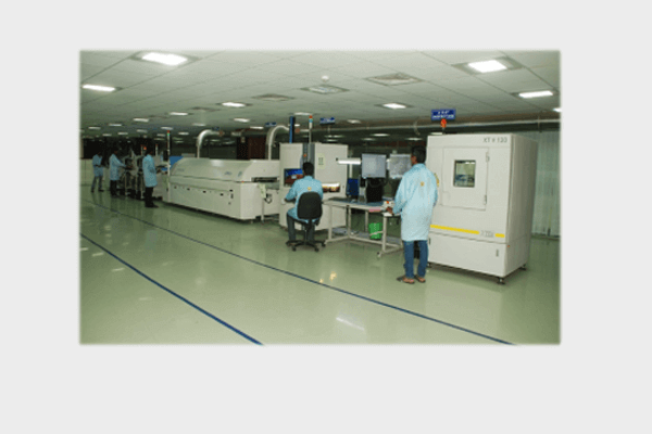
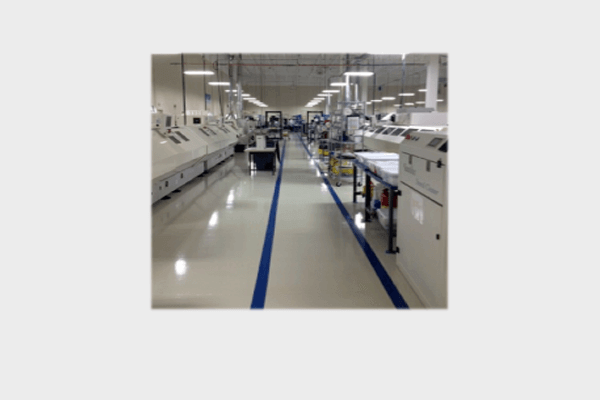
With more than 8 assembly* lines, the PCBA facilities in Bangalore, Chennai and Atlanta provide highly complex PCB assemblies with very high yield.
Sienna’s PCB assembly facilities are future ready providing support on next generation chip mounting capabilities.
Prototype Build
Complexities Handled
- PCB Thickness : upto 4.1 mm
- PCB Layers handled : 24 Layers
- POP (Package on Package assembly): 0.4mm & 0.6mm pitch
- BGA’s: Pitch - 0.4mm ,
Ball Size - 0.2, No of Balls - 2800
- QFP’s - Pitch: 0.38mm
- Discrete Packages: Up to 01005( 0.14mm X 0.20mm)
- Place component package 0201 at 45degree angle.
- 52 BGAs in an Assembly
- Max Components / PCBA : 10k
PCB Assemblies
- Hi-Complex double-sided PCB assembly
- High Mix, Low to medium volume assemblies
- ROHS and conventional process
- SMT, Through-Hole and mix technology assemblies, Backplanes
- Automated Optical Inspection (AOI)
- Design for manufacturability reviews and Yield analysis
- IPC Standards Class 2 and Class 3, MILSPEC
- In-Circuit and Flying probe test
- Latest component technologies
- Conformal coating, Encapsulation
- Total traceability